
Module 01Locked
Foundations of Semiconductor Packaging
Materials, package families, and the physics of die attach.
4 lessons
0% complete
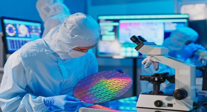
LAB 01
Hands-on training in chip packaging, PCB assembly, VLSI fundamentals and failure analysis — aligned with India's National Semiconductor Mission and PLI Scheme for electronics.
Start here
Enrol to unlock 16 lessons across 4 modules.
Curriculum
Materials, package families, and the physics of die attach.
0% complete
From schematic capture to a manufacturable, signal-integrity-clean board.
0% complete
Build a board on real lines and rework BGAs without damage.
0% complete
Find defects fast, then trace them to root cause.
0% complete
Your learning journey
Focus areas
Equipment & toolchain
Learner outcomes
Industry partners
Final assessment
60 min · 30 questions · pass mark 70% · 3 attempts · unlocks certificate
We use cookies to improve your experience
Essential cookies keep the site working. With your permission, we also use analytics cookies to understand what content is helpful and improve it. Read our privacy policy.
Install app
Add TCLMS360 to your home screen
One tap — learn offline, quick launch and a full-screen experience.