All Centres of Excellence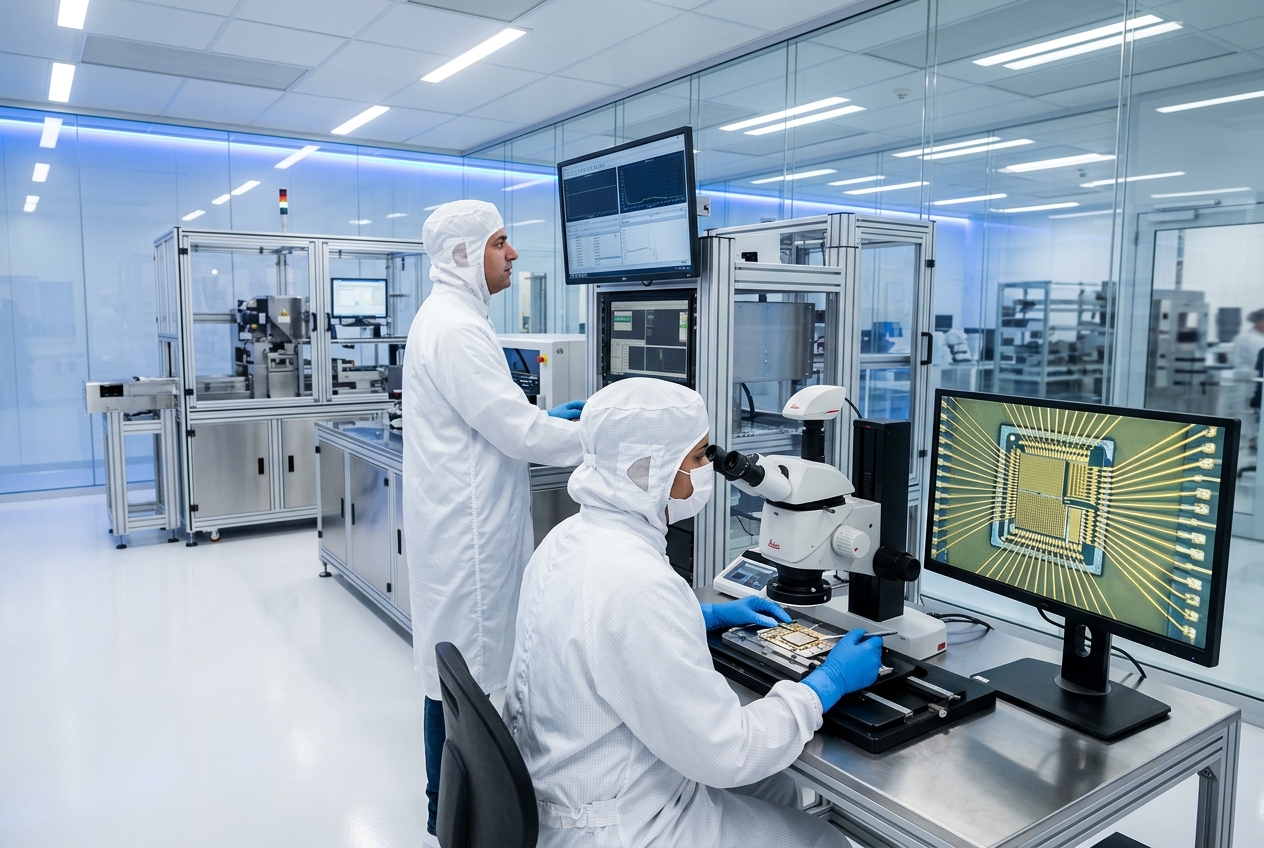
SMPL · Centre of Excellence
Semiconductor & Microelectronics Packaging Lab
India's chip-packaging muscle, built lab-side.
Why it matters
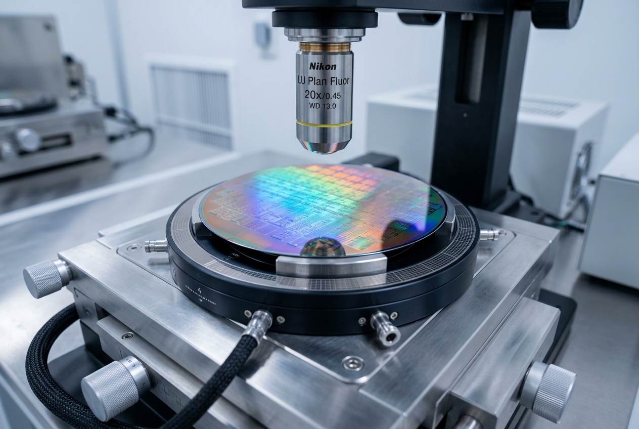
Under the India Semiconductor Mission, the country is committing close to ₹76,000 crore to attract fabs and OSAT (assembly, testing, packaging) capacity. The packaging stage alone will employ several lakh engineers over the next decade — but the talent pipeline does not exist at the depth India needs. SMPL is purpose-built to close that gap with wafer-level inspection, die-attach, wire-bond, encapsulation and electrical-test capability that mirrors the OSAT shop-floor.
What you learn here
- Wafer-level inspection and die-attach simulation
- Wire-bond and flip-chip assembly training
- Encapsulation, package-level reliability and burn-in
- Hands-on OSAT process certification for engineering graduates
Inside the lab
A look at the facility
Technology Enablers


Keep exploring